(China (Mainland))

Product Summary
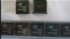
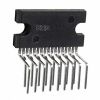
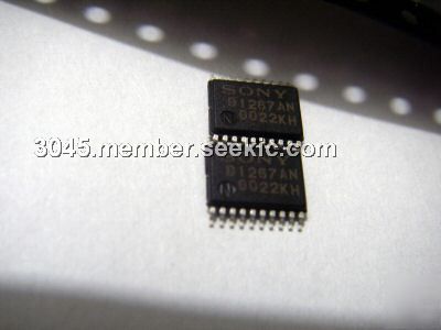
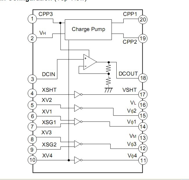
The CXD1267 is a vertical clock driver for CCD image sensor. This IC is the successor of the CXD1250N with attractive features. Power consumption is reduced approximately 30% for the CXD1267AN version.
Parametrics
CXD1267 absolute maximum ratings: (1)Supply voltage VL: 0 to –10 V; (2)Supply voltage VH VL: – 0.3 to 2VL + 35 V; (3)Supply voltage VM VL: – 0.3 to 3.0 V; (4)Input voltage VI VL: – 0.3 to VH + 0.3 V; (5)Output voltage (V2, V4)MVf VL: – 0.3 to VM + 0.3 V; (6)Output voltage (V1, V3)HVf VL: – 0.3 to VH + 0.3 V; (7)Output voltage (VSHT)HHVf VL: – 0.3 to VH + 0.3 V; (8)Operational amplifier output current IDCOUT: ±5 mA; (9)Operating temperature Topr: –25 to +85 °C; (10)Storage temperature Tstg: –40 to +125 °C.
Features
CXD1267 features: (1)Substrate voltage (Vsub)generator is built-in; (2)Variable Vsub in the range of 4.0V to 18.5V; (3)Reduction of peripheral parts saves space; (4)Only two power supplies (+15V and –8.5V)are needed; (5)3.3V clock interface is acceptable; (6)20-pin SSOP package is used; (7)Low power consumption: 62mW.
Diagrams
| Image | Part No | Mfg | Description |  |
Pricing (USD) |
Quantity | ||||
|---|---|---|---|---|---|---|---|---|---|---|
 |
 CXD1267 |
Other |
|
Data Sheet |
Negotiable |
|
||||
|
CXD1267AN |
Other |
|
Data Sheet |
Negotiable |
|
||||